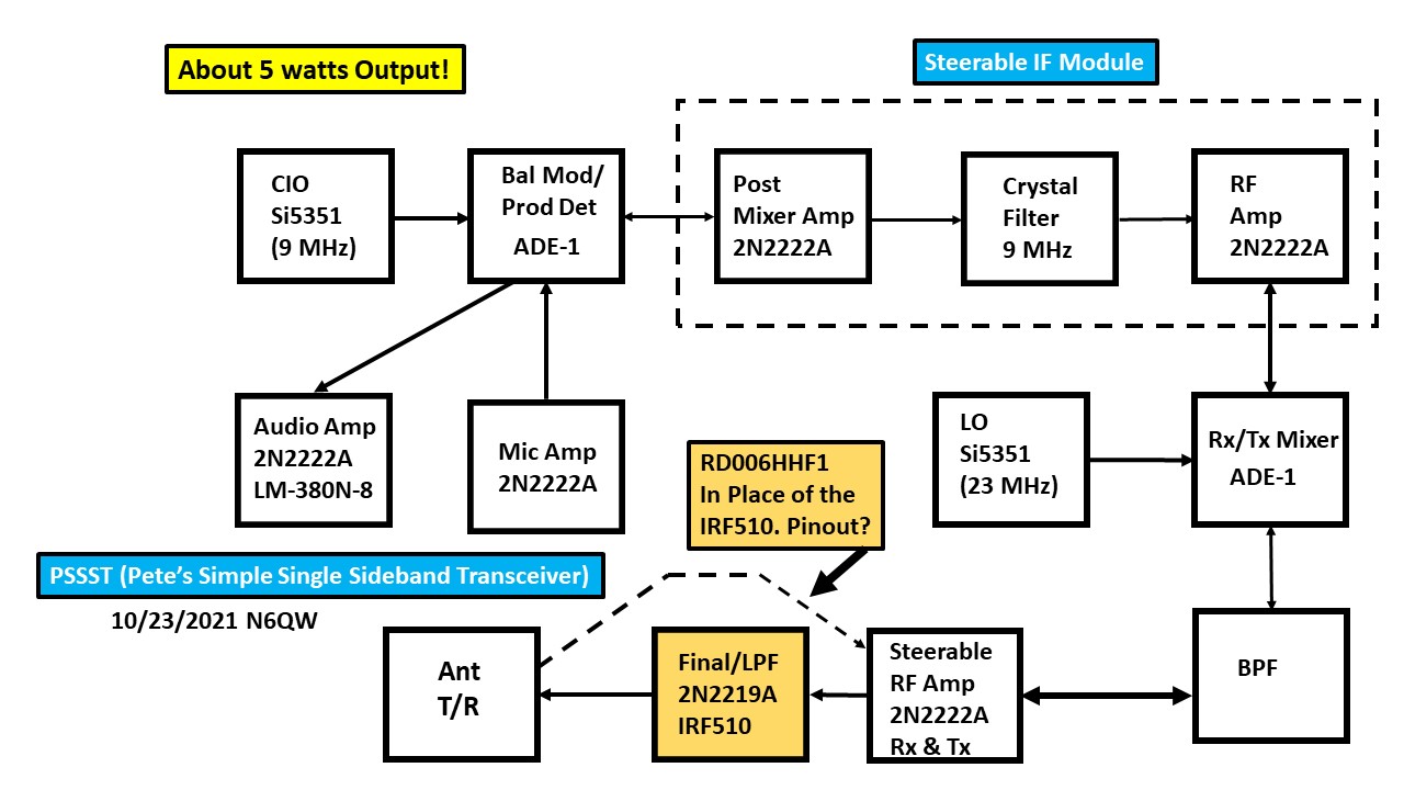
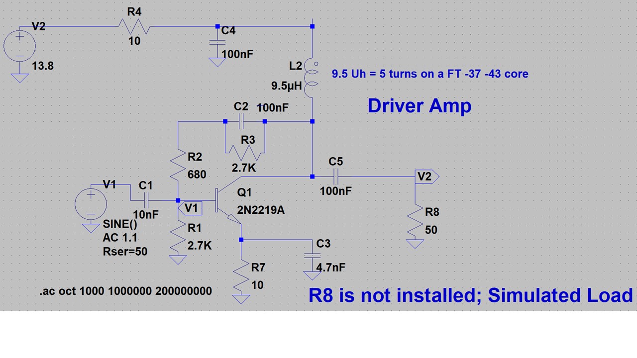
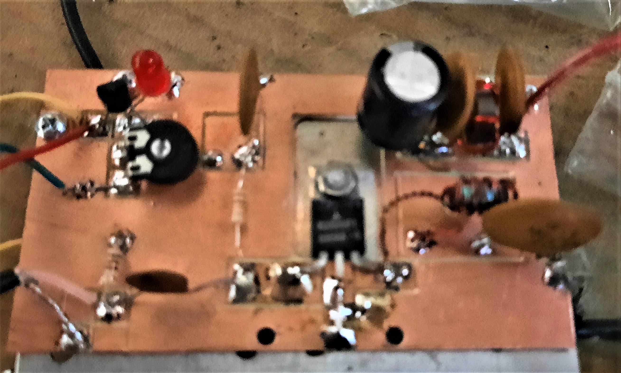
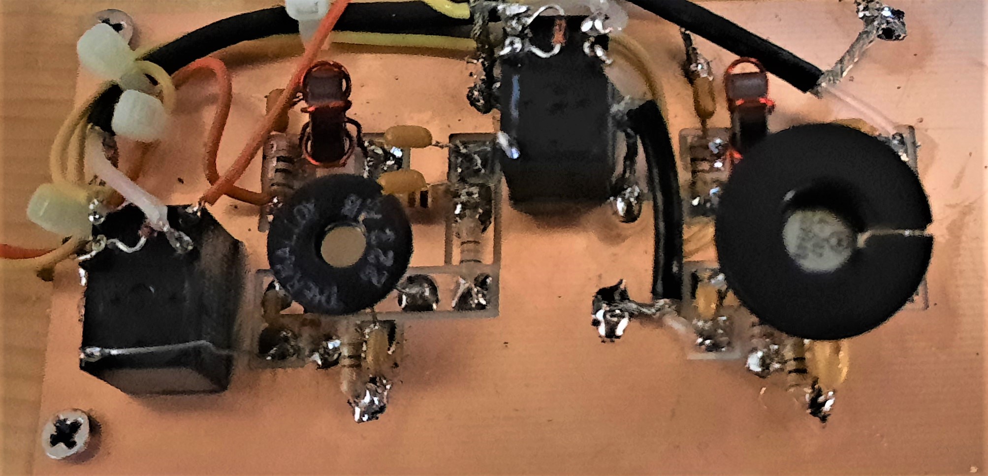
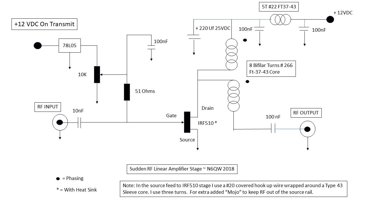
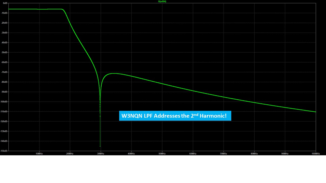
The Driver and Final Amplifier Stages These are perhaps better known as the "Grief Stages" as often they cause the most grief when trying to build a transceiver. I can't tell you how many times when 20% of a project is spent on the earlier modules and getting them working, whereas the Driver and Final are only 20% of the hardware but consume 80% of the time to get them tamed. [We have a Pareto Principle at work here and we are not talking about rabbits.] This often is the result of trying to get as much power output as possible with the minimum number of stages. High gain over driven amps are ripe for oscillation. That said by adopting some standard layouts for these stages you can get a leg up on making them behave properly. The Drivers stage uses the very same pad layout as the steerable Rx/Tx stage used as in the RX RF Amp and the Tx Prediver so I won't repeat here. However there are some minor circuit changes to drive the pants off the 2N2219A. In our write up we clearly stated and showed that the two deivces are essentially the same. But with the T0-39 case style of the 2N2219A you can get a higher device dissipation over the TO-18 case on the 2N2222A. We will show that circuit diagram. No my instincts tells me I will get emails where is the layout for the Driver --spoon feeding again! In the photo link you will see the Driver next to the Steerable amplifier . Early on I started with the IRF510 which worked OK; but upon rigorous measurement found we were only getting about 2.5 watts out. The 1st contact to Canada was made at that power level. I have since switched over to the Mitsubishi RD006HHF1 (about 5X the cost of the IRF510, $5 versus $1) but I now get about 4 watts out. Important NOTE: There are those who delight in picking apart my designs and will jump on the schematic for the IRF510 regarding the note about use in the Sudden Transceiver. Yes I recycle designs and if something works, I use it over and over and this IRF510 Amp is no exception. BTW the Sudden was a published article in the GQRP SPRAT. The pad layout I will show can accept either device BUT not the same pinout. The IRF510 from (facing up) left to right is G, D, S. The RD006HHF1 is G, S and D. The huge difference is that you need an insulator kit for the IRF510 whereas the RD006HHF1 -- screw it down to the chassis just use some heatsink compound. I used the pad layout which is shown but added the parts to it to show what parts go where on the pads. I know this by heart (my design) but other won't. Now the pad for the IRF/RD is actually cut through the PC board as that is where you make an attachment to a heat sink either through an insulator with the IRF510 or directly with the RD006HHF1. So if using the MePads just leave an open space. If you are using a CNC after cutting the initial board, go back and "hog out" (machining term) the area for the RF device. The RF Linear Amp Board has an interesting mod not shown on the schematic and needed if you use the RD006HHF1 and that is an LED. By lifting the ground Pin of the LM78L05 from ground and installing a LED between the Pin and actial ground--when you key the Bias the LED lights -- cool way to know the Amp is "ON". But more importantly it sets a threshold level so that the LM78L05 now puts out a regulated 6 VDC not 5 VDC. The RD006HHF1 can run with a higher Bias. But if you use the max Bias with the IRF510 --you will smoke. Don't say I did tell you that would happen. Information is also provided for the W3NQN LPF whihc addresses the 2nd Harmonic content
|
|---|